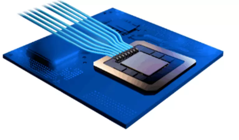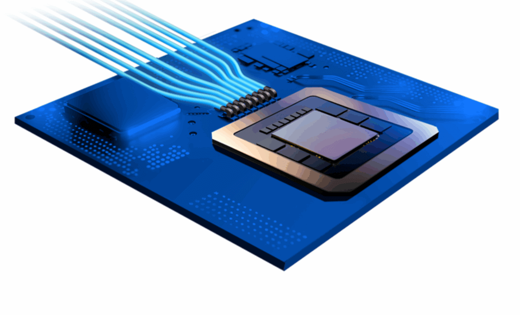
Avicena, a privately held startup based in Sunnyvale, California, announced a collaboration with TSMC to optimize photodetector (PD) arrays for its LightBundle microLED-based optical interconnects. The effort aims to extend ultra-high-density die-to-die (D2D) and processor-to-memory (P2M) optical links beyond 10 meters with energy efficiency below 1 picojoule per bit—drastically improving the scalability and power performance of AI infrastructure.
LightBundle interconnects leverage Avicena’s proprietary microLED arrays as transmitters and CMOS-bonded silicon PD arrays as receivers, achieving over 1 Tbps/mm of shoreline density. These optical transceivers are designed for flexible deployment in co-packaged optics (CPO), on-board optics (OBO), and pluggable module formats, overcoming the limitations of traditional copper-based interconnects in high-radix AI clusters and memory fabrics.
TSMC brings its leading CMOS image sensor process portfolio and manufacturing expertise to the collaboration, producing visible-light-optimized photodetectors tailored for Avicena’s microLED transmission wavelengths. The partnership supports the growing need for efficient, long-reach, and low-power I/O in AI/ML workloads by enabling chiplet-based optical interconnects compatible with modern packaging technologies.
- Avicena partners with TSMC to optimize PD arrays for its LightBundle optical interconnects.
- LightBundle delivers >1 Tbps/mm shoreline density and >10m reach with <1pJ/bit energy efficiency.
- Designed for AI, HPC, and 5G use cases, supporting CPO, OBO, and pluggable optical modules.
- PD arrays are bonded to CMOS ICs using TSMC’s CIS technologies for visible-light sensitivity.
- Avicena will showcase LightBundle at the TSMC 2025 North America Technology Symposium.
“TSMC’s world-class manufacturing capabilities and deep experience in silicon optical sensors are critical for developing and producing key components of our LightBundle interconnects,” said Bardia Pezeshki, co-founder and CEO of Avicena.