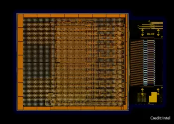
Intel is positioning advanced packaging as a central pillar of its foundry strategy, outlining how its Embedded Multi-die Interconnect Bridge (EMIB) technology can enable AI accelerators, networking silicon, and high-performance computing processors to scale well beyond the physical limits of traditional monolithic chips. In a technical blog authored by Mark Gardner, Vice President and General Manager of the Packaging and Test Business Group at Intel Foundry, the company detailed how its EMIB-T architecture addresses growing package sizes while improving manufacturing efficiency.
As AI processors increasingly rely on multiple compute chiplets and large numbers of High Bandwidth Memory (HBM) stacks, conventional 2.5D approaches based on full silicon interposers face growing economic and manufacturing challenges. Intel argues that large interposers consume significant silicon area and can reduce wafer utilization as package footprints expand. EMIB-T instead uses small embedded silicon bridges positioned only where high-bandwidth die-to-die connectivity is required. The architecture incorporates Through-Silicon Vias (TSVs) to improve power delivery while relying on an organic substrate for the majority of the package structure. Intel states that the smaller bridge approach can achieve approximately 90% wafer utilization compared to significantly lower utilization rates associated with large interposer designs. The company also noted support for open chiplet interconnect standards including Universal Chiplet Interconnect Express (UCIe) and Bunch of Wires (BoW).
Intel outlined an aggressive scaling roadmap for future multi-die systems. Current EMIB implementations support package footprints exceeding eight times the standard reticle size, corresponding to roughly 6,800 mm². By 2028, Intel expects to support packages exceeding twelve times reticle size, approaching 10,000 mm². The company said such configurations could integrate 16 or more HBM4 or HBM5 memory stacks interconnected through more than 30 EMIB-T bridges. Intel plans to combine EMIB-T with its Foveros 3D stacking technology, creating what it describes as an “EMIB 3.5D” architecture capable of supporting increasingly complex AI infrastructure designs.
• EMIB-T uses localized silicon bridges instead of full-package silicon interposers.
• Architecture incorporates TSVs to improve power delivery across large multi-die systems.
• Supports open chiplet interconnect standards including UCIe and BoW.
• Current capability exceeds 8x reticle size, or approximately 6,800 mm².
• Intel targets packages exceeding 12x reticle size, or roughly 10,000 mm², by 2028.
• Future designs could support 16+ HBM4/HBM5 stacks and 30+ EMIB-T bridges.
“By combining EMIB-T with Foveros 3D stacking, Intel Foundry is building a modular advanced packaging platform capable of supporting the next generation of AI and high-performance computing systems,” said Mark Gardner, Vice President and General Manager of the Packaging and Test Business Group at Intel Foundry.
🌐 Analysis: The announcement highlights how advanced packaging has become one of the semiconductor industry’s primary innovation vectors. AI accelerators are increasingly constrained not by transistor density alone, but by the ability to integrate large numbers of compute chiplets, HBM stacks, networking interfaces, and power delivery structures within a single package. As a result, packaging technologies such as Intel’s EMIB and Foveros, TSMC’s CoWoS and SoIC, and Samsung’s I-Cube and X-Cube have become strategic differentiators for AI infrastructure vendors.
🌐 Analysis: Intel’s roadmap also reflects the growing importance of heterogeneous integration and open chiplet ecosystems. Support for UCIe and BoW aligns with broader industry efforts to enable interoperable chiplets sourced from multiple vendors and process technologies. The company’s emphasis on scaling beyond traditional reticle limits comes as AI accelerator vendors seek larger memory footprints, higher bandwidth, and more flexible architectures to support increasingly demanding training and inference workloads. Intel’s recent appointment of former SK hynix CEO Seok-Hee Lee to lead advanced packaging initiatives further underscores the strategic importance of packaging and HBM integration within Intel Foundry’s long-term plans.
Source: “Intel Foundry’s Advanced Packaging Innovations Lead the Industry in Scaling Past Reticle Limits,” by Mark Gardner, Vice President and General Manager, Packaging and Test Business Group, Intel Foundry.
Recent Converge Digest Coverage Intel Foundry, Advanced Packaging, HBM, Chiplets & AI Infrastructure | ||
| Date | Article | Focus |
| Jun 2026 | Intel Appoints Seok-Hee Lee to Lead Advanced Packaging at Intel Foundry | HBM |
| May 2026 | Astera Labs Expands PCIe 6 Connectivity Portfolio for AI Infrastructure | Chiplets |
| Apr 2026 | Broadcom Advances AI Infrastructure Scale-Up and Scale-Out Architectures | Packaging |
| Mar 2026 | HyperLight and Salience Labs Highlight Optical Interconnect Requirements for AI Clusters | Optics |
| Why It Matters: AI accelerators increasingly depend on advanced packaging technologies—including EMIB, Foveros, CoWoS, SoIC, HBM integration, and chiplet interconnects—to scale performance beyond traditional reticle limits. These technologies are becoming as strategically important as process-node advances in determining AI system performance, power efficiency, and manufacturing scalability. | ||
🌐 We’re tracking the latest developments in networking silicon. Follow our ongoing coverage at: https://convergedigest.com/category/semiconductors/