
The U.S. Department of Defense awarded a contract to Intel to enable the U.S. government to access Intel’s state-of-the-art semiconductor packaging capabilities in Arizona and Oregon.
The project, which is supported by the DoD’s State-of-the-Art Heterogeneous Integration Prototype (SHIP) program, is executed by the Naval Surface Warfare Center, Crane Division, and administered by the National Security Technology Accelerator.
The second phase of SHIP will develop prototypes of multichip packages and accelerate advancement of interface standards, protocols and security for heterogeneous systems. SHIP prototypes will integrate special-purpose government chips with Intel’s advanced, commercially available silicon products, including field programmable gate arrays, application-specific integrated circuits and CPUs. This combination of technologies provides new paths for the U.S. government’s industry partners to develop and modernize the government’s mission-critical systems while taking advantage of Intel’s U.S. manufacturing capabilities.

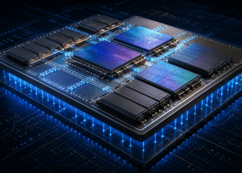
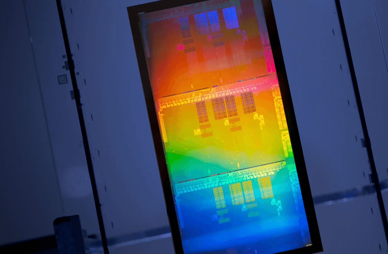
Heterogeneous packaging allows the assembly of multiple, separately manufactured integrated circuit dies (chips) onto a single package to increase performance while reducing power, size and weight. SHIP provides the U.S. government access to Intel’s advanced heterogeneous packaging technologies, including embedded multi-die interconnect bridge (EMIB), 3D Foveros and Co-EMIB (combining both EMIB and Foveros).
“Intel and the U.S. government share a priority to advance domestic semiconductor manufacturing technology. The SHIP program will enable the Department of Defense to take advantage of Intel’s advanced semiconductor packaging capabilities, diversifying their supply chain and protecting their intellectual property while also supporting ongoing semiconductor R&D in the U.S. and preserving critical capabilities onshore,” stated Jim Brinker, president and general manager of Intel Federal LLC.
“To ensure that the U.S. defense industry base can continue to deliver state-of-the-art electronics for national security, it is imperative that the Department of Defense (DoD) partners with leading U.S. semiconductor companies,” Nicole Petta, principal director of microelectronics, Office of the Under Secretary of Defense for Research and Engineering. “The DoD microelectronics roadmap recognizes the importance of strategic partnerships with industry. The roadmap also prioritizes and recognizes that as process scaling slows, heterogeneous assembly technology is a critical investment for both the DoD and our nation. SHIP directly contributes to advancing the objectives outlined in the DoD roadmap and the DoD looks forward to working with Intel, a world leader in this technology.”

In 2018, Intel demonstrated a new 3D packaging technology, called “Foveros,” which for the first time brings 3D stacking to logic-on-logic integration. Foveros will will allow products to be broken up into smaller “chiplets,” where I/O, SRAM and power delivery circuits can be fabricated in a base die and high-performance logic chiplets are stacked on top. The first Foveros product will combine a high-performance 10nm compute-stacked chiplet with a low-power 22FFL base die.