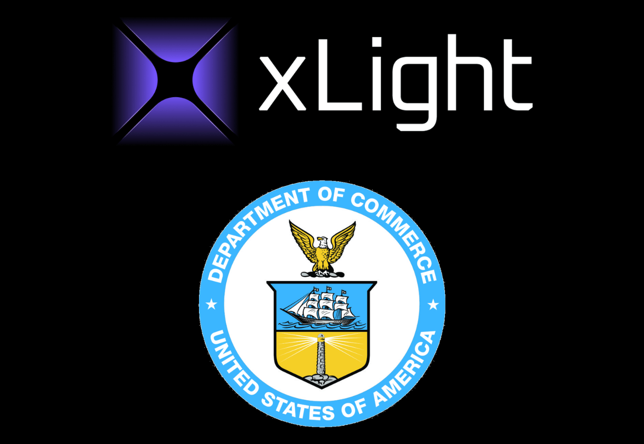
xLight has finalized a $150 million award under the U.S. CHIPS and Science Act to support construction and demonstration of its first free-electron laser (FEL) system for semiconductor manufacturing. The funding, awarded by the U.S. Department of Commerce and the National Institute of Standards and Technology (NIST), will help the Palo Alto-based company build a first-of-its-kind EUV light source platform in Albany, New York.
Founded in 2021, xLight is pursuing a different approach to extreme ultraviolet (EUV) lithography. Rather than generating EUV light inside individual lithography tools, the company aims to deploy utility-scale free-electron laser systems outside the fab and distribute EUV power to multiple scanners simultaneously. xLight says a single FEL installation could serve up to 16 lithography scanners, potentially increasing throughput, improving economics, and reducing bottlenecks in advanced semiconductor manufacturing.
The company argues that current EUV source technology may become a limiting factor as demand for advanced AI, HPC, and next-generation semiconductor devices continues to accelerate. By delivering significantly higher EUV power levels, xLight believes its FEL architecture can help expand global chip manufacturing capacity while enabling future lithography advances beyond current technology roadmaps.
- Received a final $150 million CHIPS and Science Act incentive award.
- Funding supports construction and demonstration of xLight’s first free-electron laser EUV system.
- Initial deployment is planned in Albany, New York.
- FEL systems are designed to be installed outside semiconductor fabs.
- One FEL system could provide EUV light to as many as 16 lithography scanners.
- Technology targets higher throughput, lower manufacturing costs, and expanded fab capacity.
- xLight was founded in 2021 and is headquartered in Palo Alto, California.
- The company focuses on commercializing free-electron laser technology for semiconductor manufacturing and other strategic applications.
“Lithography innovation is the key to reviving Moore’s Law,” said Nicholas Kelez, CEO and CTO of xLight. “With these incentives, the support from Commerce, and growing partnerships across the semiconductor ecosystem, xLight will deliver an EUV light source capable of powering lithography innovation for decades.”
🌐 Analysis: xLight is attacking one of the most critical constraints in advanced semiconductor manufacturing: EUV source power. Today’s leading EUV lithography systems, supplied by ASML and powered by source technology from Cymer, rely on laser-produced plasma (LPP) architectures. As semiconductor manufacturers pursue increasingly complex process nodes and High-NA EUV lithography, industry attention is turning toward next-generation source technologies capable of delivering substantially higher power levels.
| xLight Company Profile | |
|---|---|
| Company | xLight |
| Founded | 2021 |
| Headquarters | Palo Alto, California, USA |
| CEO & CTO | Nicholas Kelez |
| Focus | Free-Electron Laser (FEL) technology for semiconductor manufacturing and other strategic applications |
| Core Technology | Utility-scale Free-Electron Laser (FEL) systems for Extreme Ultraviolet (EUV) lithography |
| Key Innovation | External EUV light source capable of supplying multiple lithography scanners from a centralized laser platform |
| Target Market | Advanced semiconductor manufacturing, EUV lithography, AI and HPC chip production |
| CHIPS Act Award | $150 million (2026) |
| Project Location | Albany, New York |
| System Architecture | FEL systems installed outside the fab, delivering EUV light to as many as 16 lithography scanners |
| Mission | Commercialize free-electron lasers for critical U.S. economic and national security applications |
| Website | www.xlight.com |